A sheet of paper is about 100,000 nanometres thick. A strand of DNA is about 2 nanometres wide. Nanotechnology is the science and engineering of things in that tiny world, where scientists can see, move and design matter one atom or molecule at a time. It is already inside sunscreens, phone screens and some of the vaccines given during the COVID-19 pandemic. This guide to nanotechnology and its applications explains what the word means, why the nanoscale is so strange, how the field began, where it is used, and what the risks are.
What is nanotechnology?
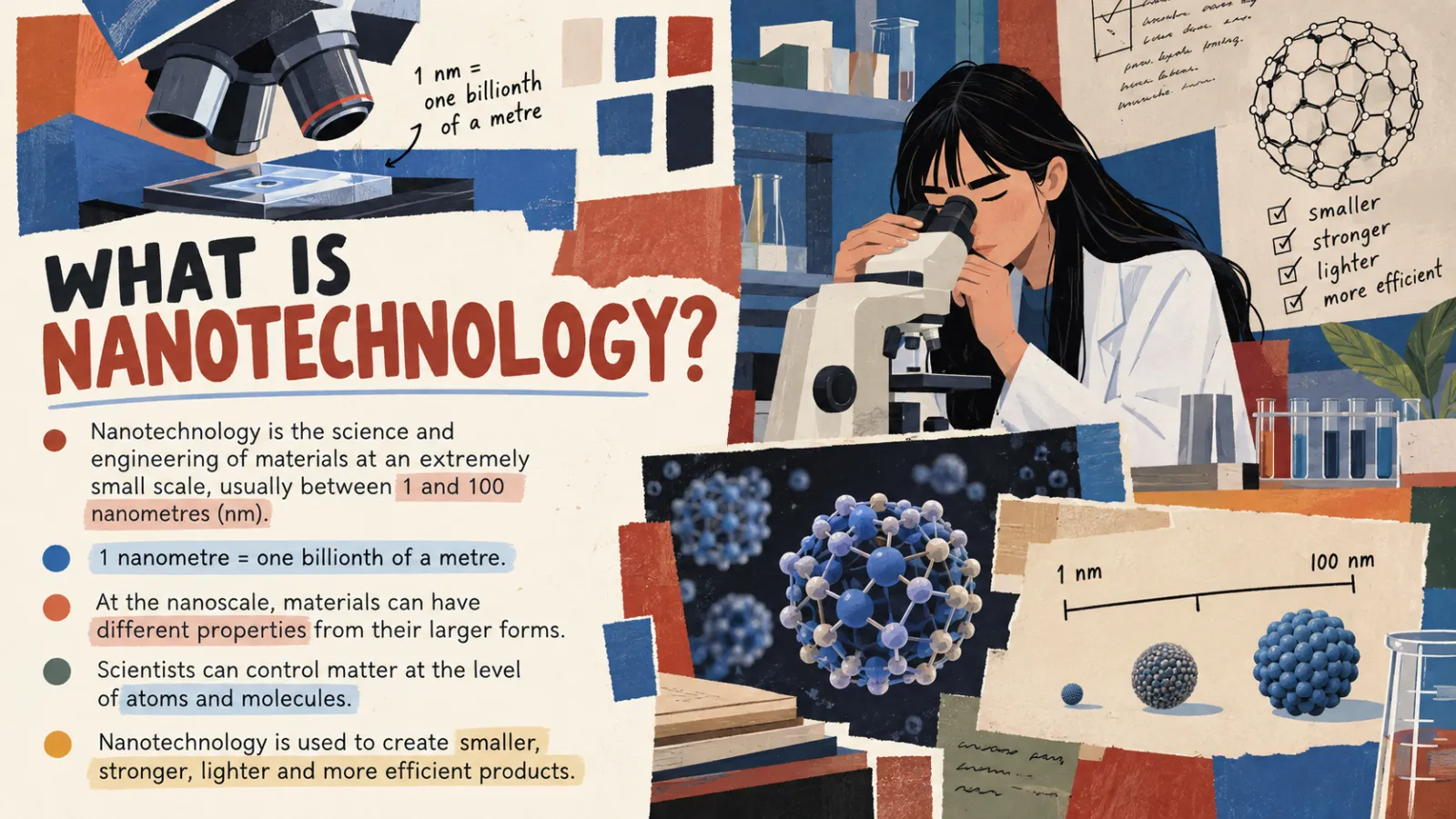
Nanotechnology is the design, production and use of materials, devices and systems with at least one dimension between 1 and 100 nm. The prefix “nano” means one billionth, so one nanometre is 10-9 m, or one billionth of a metre.
Two points are worth noticing in that definition. First, only one dimension has to be that small: a graphene sheet is huge across but about one atom thick, and still counts. Second, “nano” is not just “very small”. Below roughly 100 nm, many materials start to behave differently from the same material in larger pieces, and that is what makes the field useful.
Scientists and regulators often use that 1–100 nm range as a working definition. In 2011 the European Commission adopted a definition of a nanomaterial as a material in which 50% or more of the particles, counted by number, have one or more external dimensions in the range 1–100 nm. That Recommendation was replaced by a revised one in June 2022 (2022/C 229/01). It keeps the 1–100 nm range and the 50% by number threshold, removes the flexibility to lower the threshold, and covers solid particles only.
How small is a nanometre? A scale ladder
Numbers like 10-9 are hard to picture, so compare the nanoscale with things you know. All the sizes below are typical values rounded for easy reading; hair and paper vary a lot from sample to sample.
| Object | Approximate size | In nanometres |
|---|---|---|
| Human hair (average width) | about 0.1 mm (100 µm) | ≈ 100,000 nm |
| Sheet of paper (thickness) | about 0.07–0.18 mm | ≈ 70,000–180,000 nm |
| Red blood cell | about 7 µm | ≈ 7,000 nm |
| Upper limit of the nanoscale | 0.1 µm | 100 nm |
| DNA double helix (width) | 2 nm | 2 nm |
| Buckminsterfullerene (C60) | 0.7 nm | 0.7 nm |
So a red blood cell is about 70 times wider than the 100 nm upper limit, and a hair is about 1,000 times wider. Going the other way, the nanoscale runs down to the size of single molecules. A C60 molecule is about 0.7 nm across, only a few times wider than an atom and tiny compared with a cell.
A short history of nanotechnology
The big ideas of nanotechnology are older than the word, and the field grew as better tools made the nanoscale visible. Here are the key moments.
- 1959 – the vision. On 29 December 1959, physicist Richard Feynman gave a talk to the American Physical Society at Caltech called “There’s Plenty of Room at the Bottom”. He asked what would happen if scientists could arrange individual atoms. He offered two $1,000 prizes. One was for a tiny working motor, won in November 1960 by William McLellan. The other was for shrinking text so far that the whole Encyclopaedia Britannica would fit on a pinhead. In 1985 Tom Newman, a Stanford graduate student, won it by writing the first paragraph of A Tale of Two Cities at that scale.
- 1974 – the name. Norio Taniguchi was the first to use the term “nano-technology”, though it was not widely known at the time.
- 1981 – seeing atoms. Gerd Binnig and Heinrich Rohrer built the scanning tunnelling microscope (STM) at IBM Zurich. It can image surfaces in detail finer than 0.1 nm, and the pair received the 1986 Nobel Prize in Physics.
- 1985 – a new form of carbon. Harry Kroto, Richard Smalley and Robert Curl discovered fullerenes, including the football-shaped C60. They shared the 1996 Nobel Prize in Chemistry.
- 1986 – popular science. K. Eric Drexler published Engines of Creation, which brought nanotechnology to a wide audience.
- 1991 – nanotubes. Sumio Iijima of NEC published his work on carbon nanotubes, which brought them wide attention. He later won the first Kavli Prize in Nanoscience in 2008.
- 2004 – graphene. Andre Geim and Konstantin Novoselov isolated graphene at the University of Manchester using a piece of graphite and sticky tape. They won the 2010 Nobel Prize in Physics.
Notice the pattern: each step depended on a new way to observe or make things at the nanoscale. Understanding why the nanoscale behaves differently, and how scientists exploit that, is the topic of the next part.
If you want a deeper look at what stands in the way of using nanomaterials safely and cheaply, our article on the challenges of nanomaterials and nano designs covers it in detail.
Why does the nanoscale behave differently?
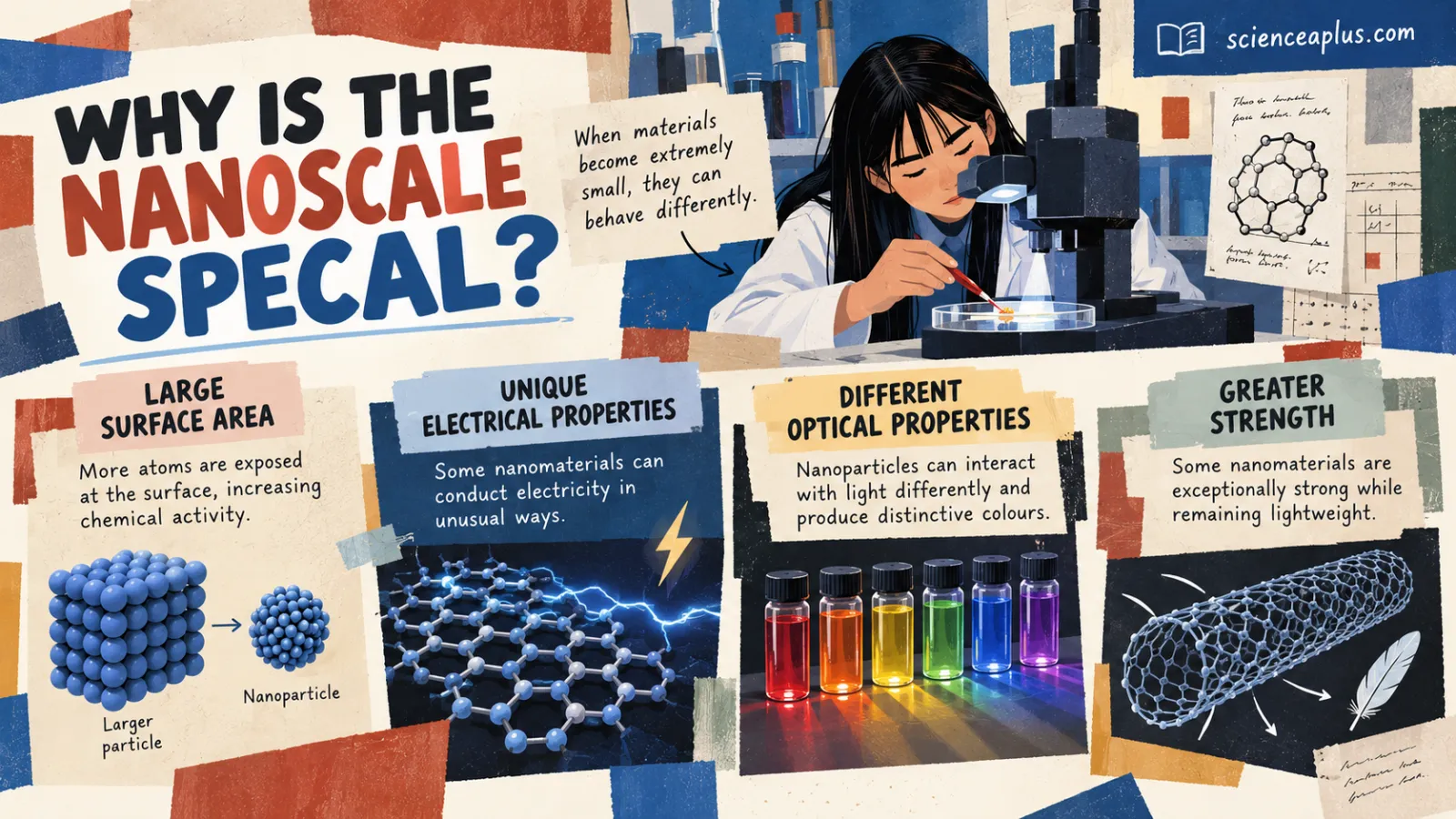
Gold is a good example. A gold ring is yellow and almost unreactive. Gold particles a few tens of nanometres across can look red, purple or blue in a liquid, and tiny gold particles are used as catalysts. The metal has not changed; the size has. Two ideas explain most of this: a huge surface area compared with volume, and quantum effects.
Surface area to volume ratio
This idea links directly to GCSE chemistry and biology. Atoms on the surface of a particle can react with their surroundings, while atoms buried inside cannot. So the more surface a given amount of material has, the more reactive and useful it can be.
For a cube with sides of length L, the surface area is 6L² and the volume is L³. Dividing gives the surface area to volume ratio:
SA : V = 6L² ÷ L³ = 6 ÷ L
Halve the side length and the ratio doubles. Shrink the cube by a factor of 10 and the ratio is 10 times larger. Here is a worked example using one cubic centimetre of material:
- A single 1 cm cube has a surface area of 6 cm² and a volume of 1 cm³, so SA:V = 6 per cm.
- Cut it into 1 mm cubes. You now have 1,000 cubes, each with a surface area of 6 mm². The total surface area is 6,000 mm², which is 60 cm². The volume has not changed, but the surface area is 10 times bigger.
- Cut it into 1 nm cubes (a thought experiment: real particles are never this perfect). The total surface area is 6 × 107 cm², which is 6,000 m², for the same 1 cm³ of material.
Try it yourself with the calculator below. Pick a side length and see how fast the ratio climbs as the particle shrinks.
A cube has sides of 5 nm. What is its surface area to volume ratio? (2 marks)
SA = 6 × 5² = 150 nm²; V = 5³ = 125 nm³. SA:V = 150 ÷ 125 = 1.2 per nm. (Quick check: 6 ÷ 5 = 1.2.)
Why does a 10 nm cube have a larger SA:V than a 100 nm cube? (1 mark)
SA:V = 6 ÷ side length, so the smaller cube has a ratio 10 times larger (0.6 per nm compared with 0.06 per nm).
Quantum effects
At the scale of a few nanometres, electrons are squeezed into a space comparable with their own wavelength, and the rules of quantum physics become obvious. The energy levels available to the electrons depend on the size of the particle.
A clear example is the quantum dot, a semiconductor crystal only a few nanometres across. Larger dots of about 5–6 nm emit orange or red light, while smaller ones of about 2–3 nm emit blue or green light. Same material, different size, different colour. The 2023 Nobel Prize in Chemistry recognised work on quantum dots, and they are used to improve the colours of some TVs.
The unusual optical, electrical and strength properties in the nanoscale can be summed up like this:
- Optical: particles can scatter, absorb and emit light differently, so size changes colour.
- Electrical: some nanomaterials, such as graphene, conduct electricity very well.
- Mechanical: some carbon nanostructures are very strong for their weight.
- Chemical: a large surface area makes catalysis and adsorption more effective.
How do scientists see and move atoms?
Ordinary light microscopes cannot show things smaller than about the wavelength of visible light (roughly 400–700 nm), so nanotechnology relies on other tools.
- Scanning tunnelling microscope (STM): a sharp conducting tip moves just above a surface, and electrons “tunnel” across the gap. The size of the tiny current reveals the surface in detail finer than 0.1 nm.
- Atomic force microscope (AFM): a very fine tip is dragged across a surface and the bending of the tip is recorded, like a record player stylus feeling the grooves.
- Electron microscopes: beams of electrons replace light, and because electrons have far shorter wavelengths, they can reveal nanoscale structures.
Carbon at the nanoscale
Carbon is the star of nanotechnology because the same atoms can be arranged in several ways with very different properties. For the basics of the element itself, see our page on carbon. Tap each card below to flip it.
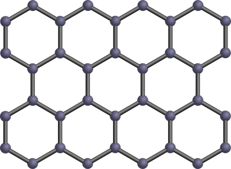
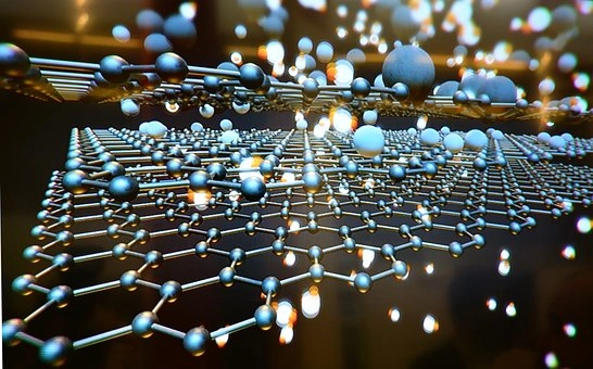
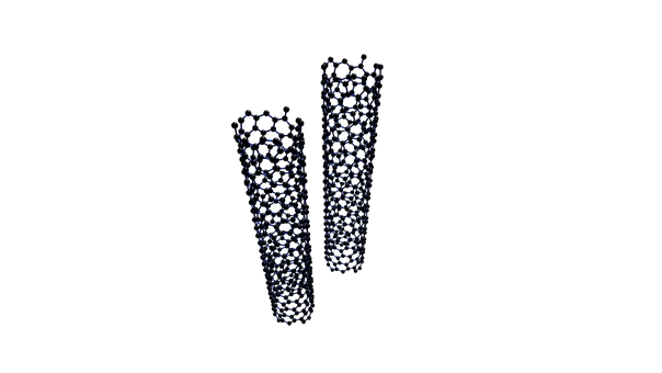

Graphene absorbs only about 2.3% of visible light even though it is one atom thick, so it is nearly transparent. Measured tensile strengths for graphene are around 130 GPa, and for an individual multi-walled carbon nanotube up to about 63 GPa (tested in 2000). Those numbers are reported for tiny, near-perfect samples. Turning that strength into everyday products at a low price is the challenge, not the science.
Nano in nature: the lotus effect
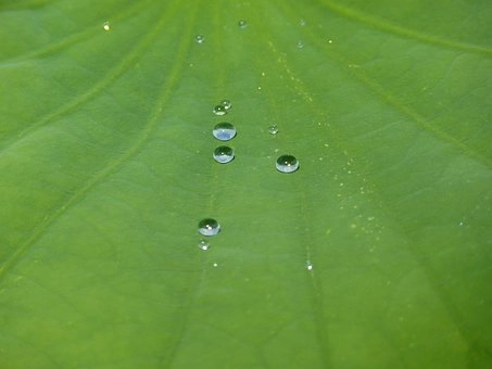
Nature has used nanoscale structures for far longer than humans have. Lotus leaves stay clean because their surface has tiny bumps and a waxy coating that make water roll up into beads. The beads pick up dust and dirt as they roll off, which is called the lotus effect. Engineers copy this idea to design self-cleaning and water-repellent surfaces.
Cells are also full of nanoscale machinery. Many structures inside cells, such as protein complexes and ribosomes, work at this scale. A whole cell, though, is far larger than the nanoscale: a red blood cell is about 7,000 nm wide.
The same ideas are used to clean up pollution. Our article on how nanotechnologies help to clean toxic waste explains how nanoparticles with a large surface area can be used to trap or break down contaminants.
Applications of nanotechnology
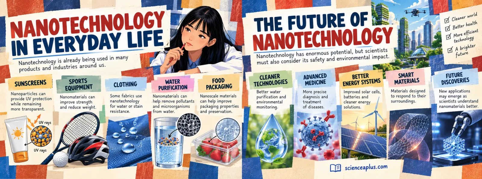
Nanotechnology is not one product but a set of methods used across many industries. Some applications are everyday and well established. Others are still being tested in laboratories, so it is worth separating what exists today from what is only promised.
Nanotechnology in medicine
Medicine is one of the most active areas of nanotechnology. The idea is to build particles about the same size as the biological molecules they need to work with, so they can carry a medicine to where it is needed. Our longer guide to the uses of nanotechnology in medicine goes into more detail.
Lipid nanoparticles and mRNA vaccines
The best-known example is the lipid nanoparticle (LNP). The Pfizer-BioNTech and Moderna COVID-19 vaccines both use LNPs to wrap and carry mRNA, the genetic instruction that tells cells how to make a harmless piece of the virus. The fatty (lipid) coat protects the fragile mRNA and helps it get inside cells. Lipid-based nanoparticles are typically between 10 and 1,000 nm across, and those used in vaccines are generally around 100 nm.
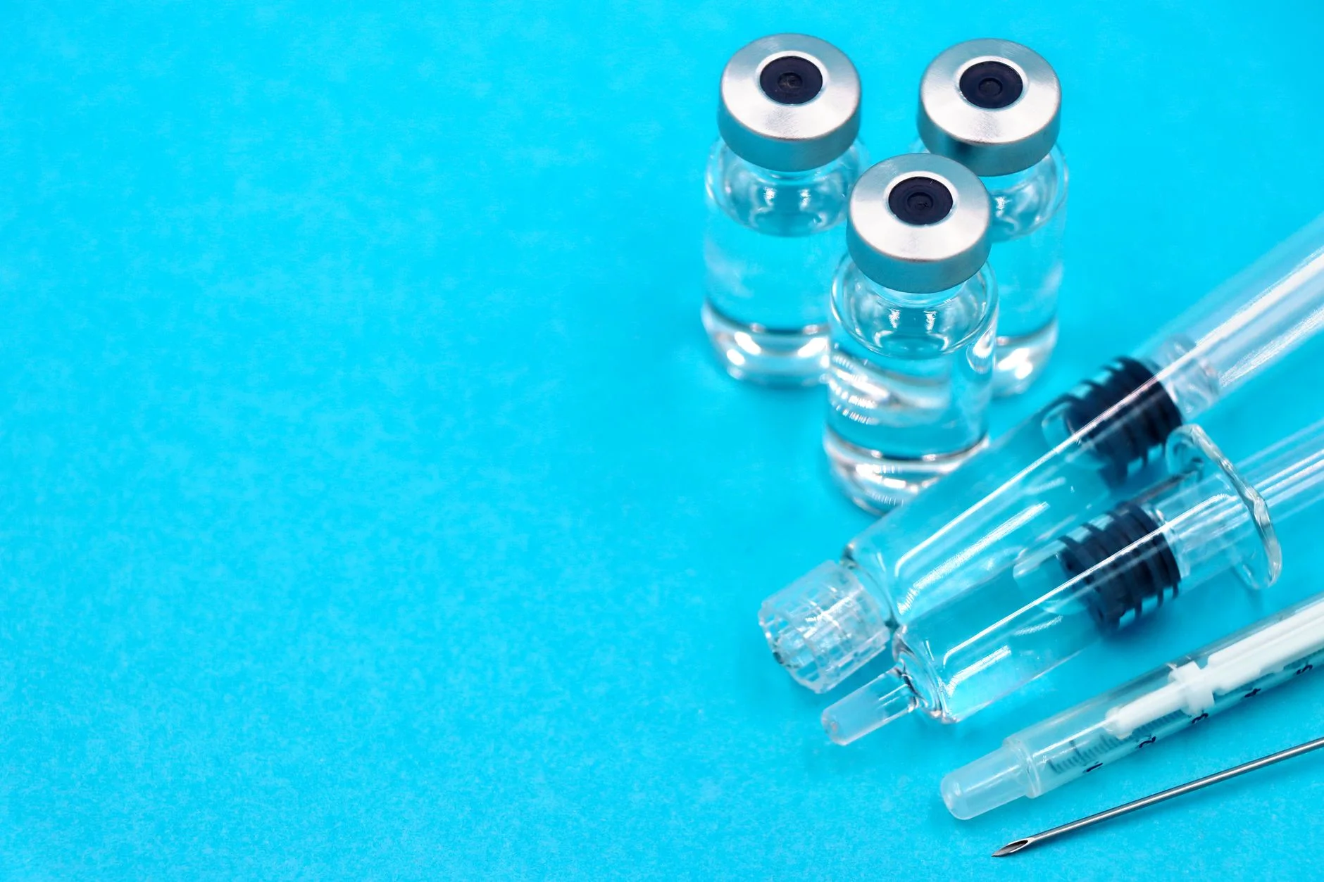
Vaccines were not the first use. In 2018 a drug called Onpattro (patisiran) was approved in the USA and the European Union. It was the first approved medicine based on small interfering RNA, and it uses lipid nanoparticles to deliver its active ingredient to the liver, treating nerve damage caused by a rare inherited condition, hereditary transthyretin amyloidosis.
Other medical uses
- Targeted drug delivery: researchers are designing nanoparticles that carry a medicine towards particular cells, with the aim of reducing side effects. Many designs are still at the research or clinical-trial stage.
- Diagnostics: gold nanoparticles are used in some rapid tests, because their colour changes in a way that can be seen.
- Wound dressings: some dressings contain silver nanoparticles, which damage bacteria. Particles with an average size of 10 nm or less seem to be the most active.
- Tissue engineering: nanostructured scaffolds are being investigated to help cells grow and repair tissue.
Looking further ahead, our article asking can nanomedicine extend the human lifespan? discusses some of these ideas and where the evidence stops.
Nanotechnology in electronics
Computers and phones rely on transistors, tiny switches made of silicon. Making them smaller lets more fit on a chip, which is why phones keep getting more powerful. Transistors are now so small that their parts are measured in nanometres, which is why electronics is often the first example people think of.

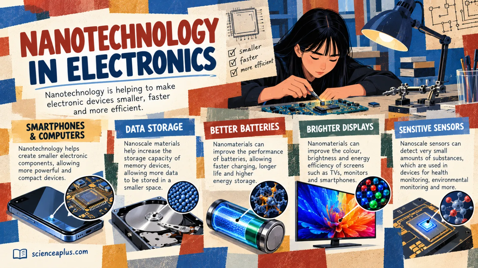
Nanotechnology also appears in other parts of electronics. Quantum dots are used to tune the colours of some screens. Researchers are developing nanomaterials for batteries, aiming for faster charging and longer life. And nanoscale sensors can detect very small amounts of a substance, which is useful for health and environmental monitoring. As with any new battery or screen technology, results vary between laboratory prototypes and mass-produced products, so claims should be treated with care.
Sunscreens, cosmetics and clothing
Sunscreen is a good everyday example of why nano size matters. Zinc oxide and titanium dioxide reflect, scatter and absorb ultraviolet light. Big particles of these white minerals leave a visible white film on the skin, but nano-sized versions can be made so that the sunscreen is far less white, while still protecting. (You can read about the metal itself on our titanium properties page.)
The NHS advice for choosing a sunscreen is to use at least SPF 30, with at least 4-star UVA protection, and to reapply every 2 hours. The particle size inside the bottle is much less important than using enough sunscreen, applying it properly and keeping out of the strongest sun.
Other consumer uses include stain-resistant and water-repellent fabrics, which copy the lotus effect, and silver nanoparticles added to some textiles to reduce odour-causing bacteria. Silver is a concern if it washes into wastewater, because it can harm the useful bacteria in treatment works.
Materials, energy and water
Adding nanomaterials such as carbon nanotubes or graphene to plastics, metals and coatings can make materials stronger or lighter, or help them conduct electricity. Examples include sports equipment, aircraft parts and protective coatings. The strength of an individual nanotube is not automatically passed on to a bulk material, so the real improvement is usually more modest than the headline figures.
Energy
Many researchers are working on nanostructured materials to improve solar panels, batteries and fuel cells, because a large surface area helps chemical reactions and light absorption. If this interests you, see also whether nanomaterials can be used to reduce CO₂ emissions.
Water treatment
Water filters can use nanoscale pores or nanoparticles to trap pollutants and microorganisms. Activated carbon, for example, is full of tiny pores, and its huge internal surface area adsorbs contaminants. Special membranes with extremely small pores are used to remove dissolved substances. This is a clear case of the surface area to volume idea at work.
Test yourself: match the application to the property
Flip each card to check your answer.
Risks, safety and regulation
The same properties that make nanomaterials useful can make them hazardous. Because they are so small, some nanoparticles can cross biological barriers that larger particles cannot, and they have a large surface area to react with living tissue. Scientists who study this field are called nanotoxicologists, and their work is still developing.
What are the main concerns?
- Breathing them in. Inhalation is the exposure route of most concern. Animal studies have shown lung inflammation and scarring for some nanomaterials.
- Carbon nanotubes. Some long, rigid nanotubes have caused effects in animal studies that resemble those of asbestos, so how long and how stiff they are matters.
- Metal nanoparticles. Silver, copper and zinc nanoparticles can damage cells in laboratory studies, and silver washed into wastewater can harm useful bacteria in treatment works.
- Environment. What happens when nanoparticles from sunscreens, textiles and coatings end up in rivers and soil is still being studied.
- Unknowns. Long-term behaviour in the body and safe exposure levels are open questions for many nanomaterials.
How is nanotechnology regulated in the UK and EU?
There is no single “nanotechnology law”. Instead, nanomaterials are covered by the rules for the type of product they are used in, such as chemicals, cosmetics, food and medicines, with extra requirements for nanoforms. In the European Union, the Commission’s definition of nanomaterial (revised in 2022, replacing the 2011 version) is used as a reference: solid particles, 1–100 nm, with at least 50% of the particles by number in that range. Chemical rules known as REACH require safety data for substances, and the EU also set up the European Union Observatory for Nanomaterials (EUON) to collect public information on their safety and markets. Some member states, such as France, Belgium, Sweden and Denmark, have national registers of nanomaterials.
Cosmetics are a visible example. Sunscreen and other cosmetic products that contain nanomaterial ingredients have to follow extra rules, including labelling so that shoppers can see “nano” in the ingredient list. Great Britain follows its own version of these rules since leaving the EU. If you need the exact current rules, check the official guidance on GOV.UK or from the relevant EU body.
Because the science moves quickly, most regulators say nanomaterials should be assessed case by case. The rules vary between countries and are still evolving.
Careers in nanotechnology
There is no single “nanotechnology degree” that everyone takes. The field draws on physics, chemistry, biology, materials science and engineering, so many routes lead into it. Here are some jobs where nanoscale work is common:
- Materials scientist or engineer: designs and tests new materials such as coatings, composites and graphene-based products.
- Chemist or chemical engineer: makes and scales up nanoparticles and catalysts (see our guide to top careers in chemistry).
- Pharmaceutical or biomedical scientist: develops drug-delivery systems and diagnostics.
- Electronics and semiconductor engineer: works on chips, sensors and displays.
- Toxicologist or regulator: studies the safety of nanomaterials and writes the rules.
At GCSE, the most useful steps are strong grades in chemistry, physics and maths, then A-levels or equivalent in some of the same subjects. Later you can specialise through a degree in one of these subjects, or in a dedicated nanoscience course.
Key points to remember
Frequently asked questions about nanotechnology
What is nanotechnology in simple words?
Nanotechnology is the science of designing and using materials at the scale of atoms and molecules, usually between 1 and 100 nanometres. At that size, materials can behave differently from larger pieces of the same substance, which lets scientists create new medicines, electronics, coatings and filters.
How small is a nanometre?
A nanometre is one billionth of a metre. A human hair is roughly 100,000 nm wide, a red blood cell is about 7,000 nm and the DNA double helix is about 2 nm wide. A nanometre is only a few times wider than a single atom.
What are examples of nanotechnology in everyday life?
Everyday examples include nano zinc oxide and titanium dioxide in some sunscreens, silver nanoparticles in some dressings and textiles, quantum dots in some screens, water-repellent fabrics, and lipid nanoparticles in mRNA COVID-19 vaccines. Many of the biggest promises, such as targeted drug delivery, are still in development.
Why do materials change at the nanoscale?
There are two main reasons. Nanoparticles have a very large surface area compared with their volume, so many more atoms are exposed and can react. Also, quantum effects start to matter, so properties such as colour and conductivity depend on particle size.
What is the surface area to volume ratio?
It is the surface area of an object divided by its volume. For a cube it equals 6 divided by the side length, so a smaller cube has a larger ratio. Nanoparticles have a very high ratio, which makes them more reactive and better at tasks such as catalysis.
What is graphene and why is it important?
Graphene is a single layer of carbon atoms arranged in a honeycomb pattern. It was isolated in 2004 by Andre Geim and Konstantin Novoselov, who won the 2010 Nobel Prize in Physics. It is very thin, strong and a good conductor, so it is being tested in electronics, batteries and composites.
Are nanoparticles in sunscreen safe?
Zinc oxide and titanium dioxide are widely used mineral UV filters, and nano forms avoid a white film on the skin. Safety is judged by regulators case by case and rules for cosmetics include extra requirements. The NHS advises using at least SPF 30 with 4-star UVA protection and reapplying every 2 hours.
Are there any risks of nanotechnology?
Yes. Inhaling some nanomaterials can inflame the lungs, some long, rigid carbon nanotubes act like asbestos fibres in animal studies, and particles released into the environment may harm wildlife. Long-term effects are still being studied, so regulators generally assess each material separately.
Is nanotechnology regulated in the UK and EU?
Nanomaterials are covered by existing rules for chemicals, cosmetics, food and medicines rather than one dedicated law. The EU uses the Commission’s definition (updated in 2022; 1–100 nm, at least 50% of particles by number) as a reference and runs the EU Observatory for Nanomaterials. Rules in Great Britain are separate from those in the EU.
What careers use nanotechnology?
Careers include materials science, chemistry, chemical engineering, pharmaceutical and biomedical research, semiconductor engineering and nanotoxicology. Good GCSE and A-level results in chemistry, physics and maths are a common route in, followed by a degree in one of these subjects.